Consumer demand for faster and faster computer processing means using smaller and smaller electronic devices to power our computers. A key challenge is to maintain the activity of the ‘dopant’ atoms that modify the electrical properties of the ultra-pure crystalline silicon used to fabricate these devices.
The vast majority of the electronic devices that power today’s computers are fabricated from ultra-pure crystalline silicon (Si) laced with minute yet controllable quantities of impurities (dopants) to modify the silicon’s electrical properties. As devices get smaller, dopant concentration increases – and many dopant atoms become electrically inactive as a result of their incorporation into dopant clusters.
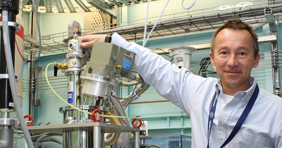 Mark Ridgway (pictured at right) from the Australian National University, Stefan Decoster from the Katholieke University Leuven in Belgium and Leandro Araujo from the University Federal Rio Grande do Sol in Brasil are using x-ray absorption spectroscopy (XAS) in collaboration with the Australian Synchrotron’s Chris Glover to deduce the atomic-scale structure of dopant clusters and identify the device fabrication conditions that minimise their formation and concentration.
Mark and his colleagues use state-of-the-art semiconductor processing technologies at the ANU’s Australian National Fabrication Facility to produce samples suitable for XAS analysis. This involves ion implantation of arsenic (As) and antimony (Sb) dopants into silicon-on-insulator wafers (Si/SiO2/Si) used for high-speed metal-oxide-semiconductor (MOS) transistor fabrication. After implantation and thermal annealing, layers of As- or Sb-doped silicon just 2 µm thick are separated from the wafer by selectively dissolving the intermediate SiO2 layer with corrosive hydrofluoric acid. If the etching procedure is successful and the researcher retains all of his/her fingers, 10 of these very fragile layers are then stacked together to create a sample for XAS analysis. This process yields a much improved XAS signal-to-noise ratio that enables the local atomic-scale surroundings of the dilute dopant to be investigated on the XAS beamline at the Australian Synchrotron.
“With its intense wiggler source and pixel-array detector technology, the XAS beamline at the Australian Synchrotron is ideally suited for ultra-dilute XAS fluorescence measurements,” Mark says. “It’s one of only a handful of beamlines in the world up to this challenge.”
The results (shown below as Fourier-transformed XAS spectra) indicate that an increase in arsenic dopant concentration increases disorder in the surrounding silicon lattice and therefore decreases the amplitude. To complement their ongoing XAS investigations, the researchers are also conducting sheet resistance measurements to probe the electrically-active dopant fraction, ion scattering measurements to probe the dopant lattice location and double-crystal x-ray diffraction measurements to probe lattice strain.
Mark and his colleagues “seek to achieve fundamental insight to yield results of not only scientific significance but also of technological importance”. For Lightspeed readers this should hopefully mean faster computers for work and play.
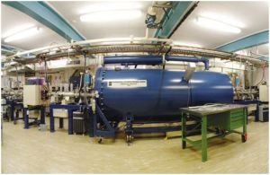
Above left: ANU’s ion implantation facility is being used to produce doped silicon samples for synchrotron analysis. Image: Mark Ridgway
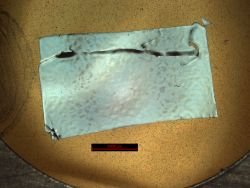
Above right: Optical micrograph of a thin layer of crystalline silicon (on adhesive Kapton) ready for XAS analysis. Image: Mark Ridgway
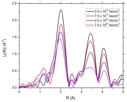
Above: Proof-of-concept: the Fourier-transformed XAS spectra (arsenic K-edge of As-doped Si) as a function of arsenic dopant concentration. Image: Mark Ridgway